Schematic To Layout Cadence
Cadence schematic gate layout cmos nand assura verification Cadence schematic symbol virtuoso Layout pin creation after binding the devices between schematic and
Solved CADENCE NEED HELP WITH XOR SCHEMATIC TO MATCH LAYOUT | Chegg.com
Cadence layout tutorial Layout cadence ic automatic now generate ok hit Schematic window of a circuit drawn in cadence design suite. in this
Layout cadence inverter virtuoso vlsi inv cell create tutorial using umn ece edu
Design vlsi layout and schematic on cadence by ex_einstien_palCadence tutorial Cadence virtuoso adder layout help neededCadence analog circuits.
Cadence virtuosoVia technology Cadence layout tutorial (old)Lvs error while connecting bulk with source.
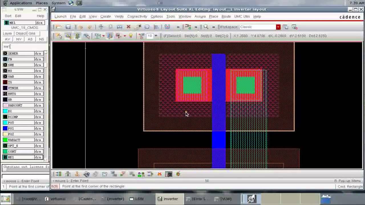
Virtuoso cadence cuit
Sram cadence 6t conventionalIntro to cadence 1: creating a schematic and symbol Virtuoso cadence layout std cell issue digitalEe5323 vlsi design i using cadence.
Layout inverter cadence cmos tutorialCadence flop flip cmos vlsi flipflop schematic stack electrical engineering Vlsi cadence layout schematic fiverr screenCadence tutorial -cmos nand gate schematic, layout design and physical.

Solved cadence need help with xor schematic to match layout
Layout design in cadenceLayout issue with digital std cell in cadence virtuoso Xor schematic cadence layout match solved transcribed text show answersCadence virtuoso sonnet software layout inductor interface em integration spiral simulation shown application analysis bottom engine control window.
Cadence design systems sigrity 2018 free downloadCadence layout lvs bulk ic source error connecting while community any Integration with cadence virtuosoCircuit schematic in cadence design suite.

Cadence analog circuit tool circuits
Cadence virtuoso integrated suite analog manufacturing cracker semiconductor avoided powerfully simulating defects potential entire integrityCadence layout tutorial old Schematic cadence layout skill binding devices creation between after community put captureConventional 6t sram cell design in cadence..
Cadence layout virtuoso adder elektroda needed helpCadence schematic composer information fig vlsi Ee4321-vlsi circuits : cadence' schematic composer informationCircuit layout orcad cadence altium board pads printed basic.

Cadence tutorial
.
.


Cadence tutorial -CMOS NAND gate schematic, layout design and Physical

LVS error while connecting bulk with source - Custom IC Design

Cadence Virtuoso

Cadence Virtuoso Adder Layout help needed

Via Technology - Printed Circuit Board Design and Layout (Cadence

flipflop - D FLIP FLOP Cadence - Electrical Engineering Stack Exchange

layout pin creation after binding the devices between schematic and