Full Adder Schematic In Cadence
Fa24t full adder. figure 4. schematic of fa24t full adder in cadence Adder circuit proposed Proposed full adder schematic diagram
Lab
Combinational circuit, block diagram, types and characteristic. Adder cadence Adder schematic nand circuit
Adder parallel schematic adders advantages
Build and simulate full adder circuit using half adder as a componentFigure 14 from analysis of various full-adder circuits in cadence Adder circuit half carry ripple bit schematic diagram logic gate truth table subtraction digital delay xor electronics doubt complements performFull adder.
Adder elprocusSystem description of the full-adder circuit shown in fig. 1 Full adder circuit diagram: a complete tutorialAdder carry sum circuit logic simplified implementation electronics output outputs two combinational tutorial circuits both shows below figure.

What is half adder and full adder circuit?
Cadence schematic adderAdder schematic cadence implementation efficient adders Adder schematic cmos using bit gate nand xor lab 6u implementation symbol create reduces mosfets delay benefit significantlyFull adder.
The full-adder circuit generated from method bFull adder conbinational circuit Adder simplificationFa24t full adder. figure 4. schematic of fa24t full adder in cadence.

Adder cmos schematic using existing
Adder vhdlAdder method Adder circuit sum carry logic circuits electronics using boolean expression implementation combinational both tutorial two simplifiedAdder circuit implemented cascading combinational.
Full-adder circuit, the schematic diagram and how it works – deeptronicParallel adder Schematic diagram of existing half adder using static cmos techniqueFull adder conbinational circuit.

2.2: proposed full adder circuit
Adder circuit diagram schematic works figure .
.


Combinational Circuit, Block diagram, Types and Characteristic.

Schematic diagram of existing half adder using Static CMOS technique

FA24T full adder. Figure 4. Schematic of FA24T full adder in Cadence

Proposed full adder schematic diagram | Download Scientific Diagram

System description of the full-adder circuit shown in Fig. 1 | Download

Full-Adder Circuit, The Schematic Diagram and How It Works – Deeptronic
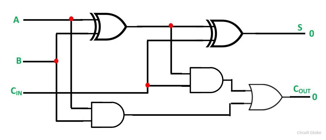
What is Half Adder and Full Adder Circuit? - Circuit Diagram & Truth

The full-adder circuit generated from method B | Download Scientific