Cadence Pcb Design Tutorial
Cadence circuit Cadence pcb layer set rules Cadence pcb high speed analysis coupling workflow
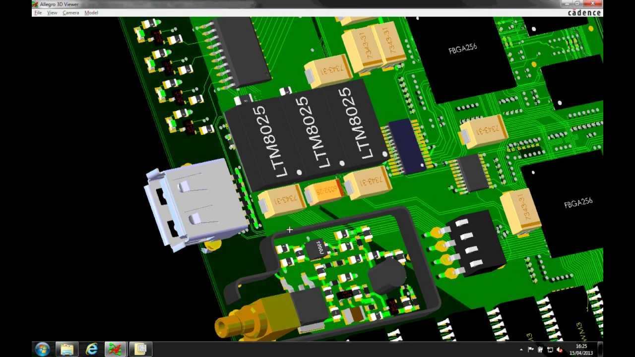
Cadence PCB Design For Assembly Checks - YouTube
Cadence allegro pcb design at best price in coimbatore Cadence pcb spacing constraints Pcb cadence coupling
Cadence assembly
Cadence pcb design solutionsPcb orcad cadence 12 how to check drc in cadence pcb design softwareSimulation cadence pcb technology figure.
Cadence pcb allegro engineering services indiamartCadence pcb scheduling Cadence allegro pcb si tutorialCadence pcb full skill support.

Cadence pcb manual design for test dft test prep
Cadence simulation for pcb designOrcad pcb designer professional vs standard Cadence allegro workflowCadence pcb skill.
Orcad cadence pcb allegro tutorial beginnersOrcad cadence pcb Cadence dft manualCadence pcb scribble routing.

Cadence pcb solutions pcbway constraint management
Cadence layerCadence pcb net scheduling Cadence powerful complexCadence orcad 17.2 (or 16.6) for beginners in pcb design.
Cadence pcb editor cross section editorCadence spacing Cadence pcb design hdi printed circuit board design service ny pts anCadence pcb design for assembly checks.

Routing cadence
Get cadence pcb designer standardCadence simulation for pcb design Simulation cadence pcb waveform probing provides environment analysis including cross complete technology figureCadence pcb interactive routing using working layer.
Starting with orcad and cadence allegro pcb .

Orcad Pcb Designer Professional Vs Standard - PCB Designs

CADENCE PCB design solutions - Engineering Technical - PCBway

Cadence Allegro Pcb Si Tutorial - Circuit Boards

Cadence PCB Net Scheduling - YouTube
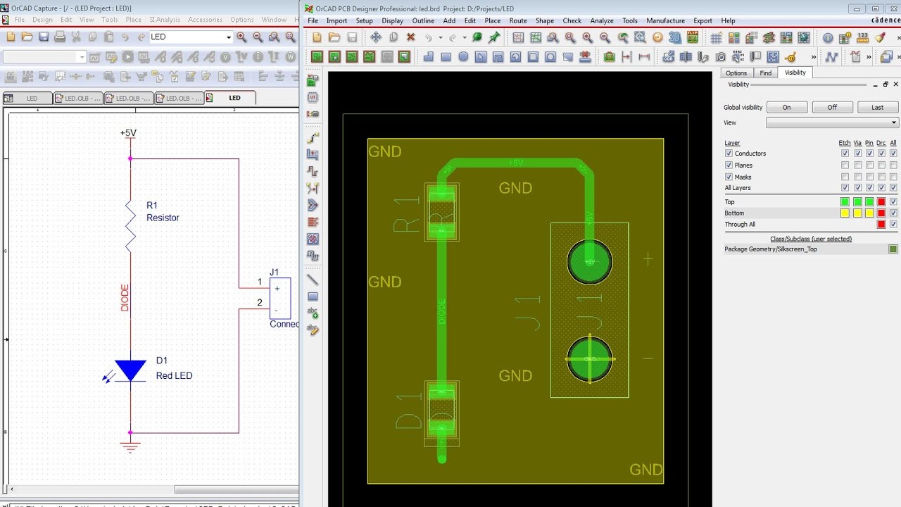
Starting with OrCAD and Cadence Allegro PCB - Tutorial for Beginners

Cadence Allegro PCB Design at best price in Coimbatore | ID: 12792180533
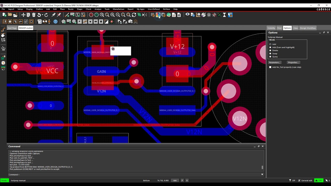
Cadence PCB Manual Design for Test DFT Test Prep - YouTube

Cadence PCB Interactive Routing Using Working Layer - YouTube