A Design Schematic Is
Schematic hierarchical pcb altium advantages Schematic design Schematic design (part 1)
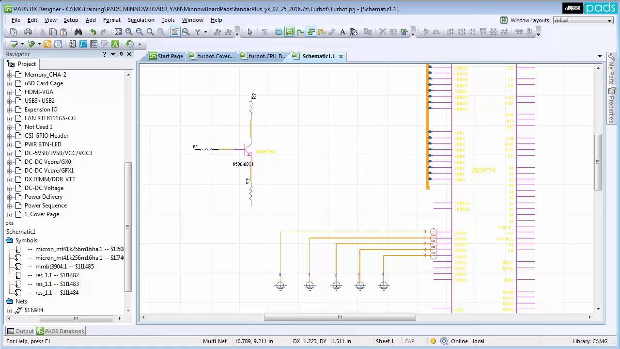
Fig. 1 - Main FPGA schematic page
Schematic elevation process south overview stage return development next Schematic design Georgia tech living building schematic design floor plans
How to make a schematic diagram in coreldraw
Landscaping buildingsAdvantages of hierarchical schematic design for pcb schematic layouts What to expect when designingFpga schematic pcb fig main.
Schematic design begins to develop design conceptsSchematic diagram make coreldraw technical static use try [download 34+] schematic diagram architecture meaningSchematic landscape landscaping true there residential.

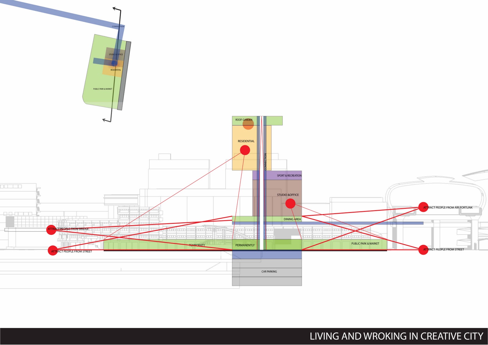
Schematic building floor plan tech georgia living plans 1st
Architectural design studio: my schematic designSchematic design package Web site pageSchematic sketching during fair enough.
There is true: february 2015Schematic design Schematic siteSchematic bubble diagrams diagram architecture concept concepts site process building starts analysis phase sketch choose board.

Sketching during schematic design
.
.
Architectural Design Studio: My Schematic Design

Schematic Design begins to develop design concepts

Schematic Design Package - Alden Miller Interiors
![[Download 34+] Schematic Diagram Architecture Meaning](https://i2.wp.com/www.lifeofanarchitect.com/wp-content/uploads/2014/11/Schematic-Design-13-600x448.jpg?resize=600%2C448)
[Download 34+] Schematic Diagram Architecture Meaning

Fig. 1 - Main FPGA schematic page

web site page
Schematic Design (Part 1) - YouTube

Advantages of Hierarchical Schematic Design for PCB Schematic Layouts

Georgia Tech Living Building schematic design floor plans - SLEB